
MTIA Series: A Technical Deep Dive
Executive Summary
Meta has unveiled four generations of its Meta Training and Inference Accelerator (MTIA) custom silicon: the MTIA 300, 400, 450, and 500. These chips are built in close partnership with Broadcom and emphasize modular chiplet designs, RISC-V vector cores, and progressively higher HBM bandwidth tailored for ranking & recommendation (R&R) workloads and generative AI inference. The MTIA 400 is described as achieving raw performance competitive with leading commercial products, while the 450 and 500 claim performance “much higher” than existing leading commercial silicon through substantial HBM bandwidth increases. Meta plans to deploy these chips at massive scale—multiple gigawatts in 2027 and beyond—while maintaining a six-month chip development cadence using reusable chassis, racks, and networking infrastructure. This announcement signals Meta’s aggressive move toward vertical integration in AI hardware to reduce reliance on merchant silicon for its enormous recommendation and generative AI workloads.
Technical Architecture
The MTIA family follows a chiplet-based, modular design philosophy that allows Meta to iterate rapidly while reusing significant portions of the system stack.
-
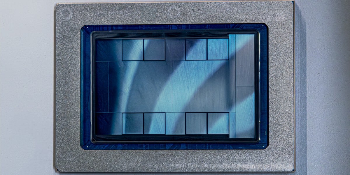
MTIA 300: Positioned as a communications-focused accelerator optimized primarily for ranking and recommendation workloads. It consists of one compute chiplet, two network chiplets, and several HBM memory stacks. The compute chiplet contains a grid of processing elements (PEs), with redundant PEs included to improve manufacturing yield. Each PE integrates a pair of RISC-V vector cores. The chip is already in production.
-
MTIA 400: An evolutionary step from the 300 that adds support for generative AI models alongside continued R&R capability. It doubles the compute resources by employing two compute chiplets. Meta states this is the first chip in the series to deliver “raw performance competitive with leading commercial products.” A full rack containing 72 MTIA 400 devices, interconnected via a switched backplane, forms a single large scale-up domain. The chip has completed testing and is “on the path to deploying” in Meta data centers.
-
MTIA 450: Purpose-built with specific optimizations for GenAI inference. Its headline architectural change is doubling the HBM bandwidth compared to the MTIA 400. Meta claims this results in performance that is “much higher than that of existing leading commercial products.” Mass deployment is scheduled for early 2027.
-
MTIA 500: Further refines the inference-focused design for efficiency. It increases HBM bandwidth by an additional 50% over the MTIA 450. The compute architecture shifts to a 2×2 configuration of smaller compute chiplets, surrounded by several HBM stacks and two network chiplets. An additional SoC chiplet provides PCIe connectivity to the host CPU and scale-out NICs. Mass deployment is planned for 2027.
A key enabler of Meta’s velocity is the reusable and modular design across chiplets, chassis, racks, and network infrastructure. The MTIA 400, 450, and 500 all utilize the same chassis, rack, and network infrastructure, significantly reducing the engineering overhead of each new generation. Meta states it now has the capacity to ship a new chip roughly every six months.
The underlying processing elements continue to rely on RISC-V vector cores, suggesting Meta is investing in a customized open-source ISA ecosystem rather than licensing high-volume Arm or x86 cores for its accelerators. The progressive increase in HBM bandwidth across the 400→450→500 sequence indicates that memory bandwidth has been identified as the primary bottleneck for Meta’s particular mix of large-scale recommendation models and generative inference workloads.
Performance Analysis
Meta has not published traditional standardized benchmarks (such as MLPerf Inference or training scores) in the announcement. Instead, the company provides qualitative and relative performance statements:
- MTIA 400: “raw performance competitive with leading commercial products”
- MTIA 450: performance “much higher than that of existing leading commercial products” due to doubled HBM bandwidth
- MTIA 500: further 50% HBM bandwidth uplift over the 450, targeting improved efficiency for GenAI inference
No absolute numbers for TOPS, TFLOPS, power consumption, or tokens-per-second are disclosed. Similarly, no direct head-to-head comparisons against specific competitors (NVIDIA H100/H200/B200, AMD MI300X, Google TPU v5, AWS Inferentia, or Groq LPU) are provided with quantitative data.
The most concrete deployment detail is the scale: a single MTIA 400 rack contains 72 accelerators connected through a switched backplane to create one large scale-up domain. This suggests Meta is building systems that can support very large embedding tables and model sharding across many devices—common in industrial-scale recommendation systems.
Broadcom has publicly stated that Meta will install “multiple gigawatts” of these chips in 2027 and beyond, indicating the total deployed power envelope will be enormous. This implies Meta expects the MTIA family to handle a significant fraction of its AI inference and recommendation traffic at hyperscale.
Technical Implications
Meta’s aggressive custom silicon roadmap has several ecosystem implications:
-
Reduced dependency on merchant AI accelerators: By developing its own inference-optimized silicon, Meta can potentially lower both capital expenditure and operating costs compared to purchasing high-margin NVIDIA GPUs for every inference task. Recommendation systems and ranking models often have different compute/memory profiles than the transformer-heavy training workloads that dominate GPU demand.
-
Acceleration of the open-source RISC-V ecosystem in AI: Heavy use of RISC-V vector cores in production hyperscale silicon validates the architecture for AI acceleration and may encourage further investment in RISC-V vector extensions and tooling.
-
Pressure on merchant silicon vendors: The announcement comes shortly after Meta signed massive deals with both NVIDIA and AMD. The existence of a competitive internal alternative gives Meta stronger negotiating leverage and creates a credible threat that could influence pricing and supply allocation from commercial vendors.
-
Infrastructure standardization: The decision to keep the same chassis, rack, and networking for three generations (400/450/500) represents a significant operational advantage. It allows Meta to treat new silicon generations more like drop-in compute upgrades rather than full rack-scale redesigns.
Limitations and Trade-offs
Several important caveats remain:
-
Lack of public benchmarks: Without MLPerf, internal tokens-per-joule, or latency/throughput numbers, it is impossible for outsiders to verify Meta’s “competitive” or “much higher” claims. History shows that vendor-specific claims often optimize for narrow internal workloads.
-
Narrow workload focus: These chips appear heavily optimized for Meta’s recommendation systems and specific generative AI inference patterns. They may not be generally programmable or competitive on diverse AI research workloads that hyperscalers such as Google, Microsoft, or Anthropic run.
-
Manufacturing and yield risk: The use of redundant PEs in the MTIA 300 and the complex multi-chiplet designs in later generations indicate yield and packaging challenges. The 2×2 smaller chiplet approach in the 500 suggests Meta is navigating reticle limits and attempting to improve yields through disaggregation.
-
Power and thermals: Multiple gigawatts of deployment implies enormous power draw and cooling requirements. While custom silicon can be more efficient than general-purpose GPUs for targeted workloads, the absolute scale Meta is targeting will stress power delivery and data center infrastructure.
-
Software ecosystem: Developing and maintaining high-performance software for a custom RISC-V-based accelerator at Meta scale is non-trivial. The company will need mature compilers, model partitioning tools, and quantization pipelines optimized for these specific PE grids.
Expert Perspective
Meta’s six-month chip cadence is remarkable and suggests the company has built a highly effective internal silicon development machine in partnership with Broadcom. The rapid iteration from MTIA 300 (R&R-focused) to the 400–500 series (progressively more GenAI-capable) demonstrates a clear understanding that memory bandwidth, not raw compute, is the dominant bottleneck for their production workloads.
The most significant aspect may be the infrastructure reuse strategy. By standardizing chassis, racks, and networking across multiple silicon generations, Meta has decoupled silicon development velocity from fleet-wide operational complexity—an advantage few other organizations can match.
While the lack of concrete performance numbers makes direct comparison difficult, the combination of “competitive with leading commercial products” on the 400 and “much higher” on the 450/500, paired with multi-gigawatt deployment plans, indicates Meta believes it has achieved a meaningful efficiency or cost advantage on its specific mix of ranking, recommendation, and generative inference tasks. If these claims hold in real production environments, this could represent one of the more successful large-scale custom AI silicon efforts outside the major cloud providers.
Technical FAQ
How does the MTIA series compare to NVIDIA or AMD accelerators on standard benchmarks?
Meta has not published any MLPerf, SPEC, or other standardized benchmark results. The company only offers qualitative statements (“competitive with leading commercial products” for MTIA 400 and “much higher” for 450/500). Direct quantitative comparison is not yet possible from public data.
What is the process technology node and exact power envelope of these chips?
These details have not been disclosed in the announcement. The focus remains on architectural description, HBM bandwidth scaling, and deployment timelines rather than process node, TDP, or transistor counts.
Is the MTIA architecture programmable for arbitrary models or narrowly optimized for Meta’s workloads?
The architecture appears heavily tailored for Meta’s ranking & recommendation systems and specific generative AI inference patterns. The use of custom RISC-V vector cores in a grid of processing elements suggests a domain-specific accelerator rather than a fully general-purpose GPU-style programmable device.
How does the six-month chip cadence impact software and firmware development?
Meta claims the reusable modular design (chiplets, chassis, rack, network) reduces the scope of changes required per generation. However, sustaining high-performance model compilation, quantization, and orchestration tools across rapidly evolving silicon revisions will remain a significant software engineering challenge.
References
- Meta official blog post on custom silicon (March 2026)
- Broadcom statements regarding multi-gigawatt Meta deployment
- Related coverage from WIRED, CNBC, Wccftech, and TechBuzz
Sources
- The Register - Meta reveals four custom AI chips
- WIRED - Meta Is Developing 4 New Chips to Power Its AI and Recommendation Systems
- CNBC - Meta rolls out in-house AI chips weeks after massive Nvidia, AMD deals
- Wccftech - Meta 'Sprays Out' Four MTIA AI Chips in Two Years
- TechBuzz - Meta Unveils 4-Chip MTIA Roadmap in 24 Months