
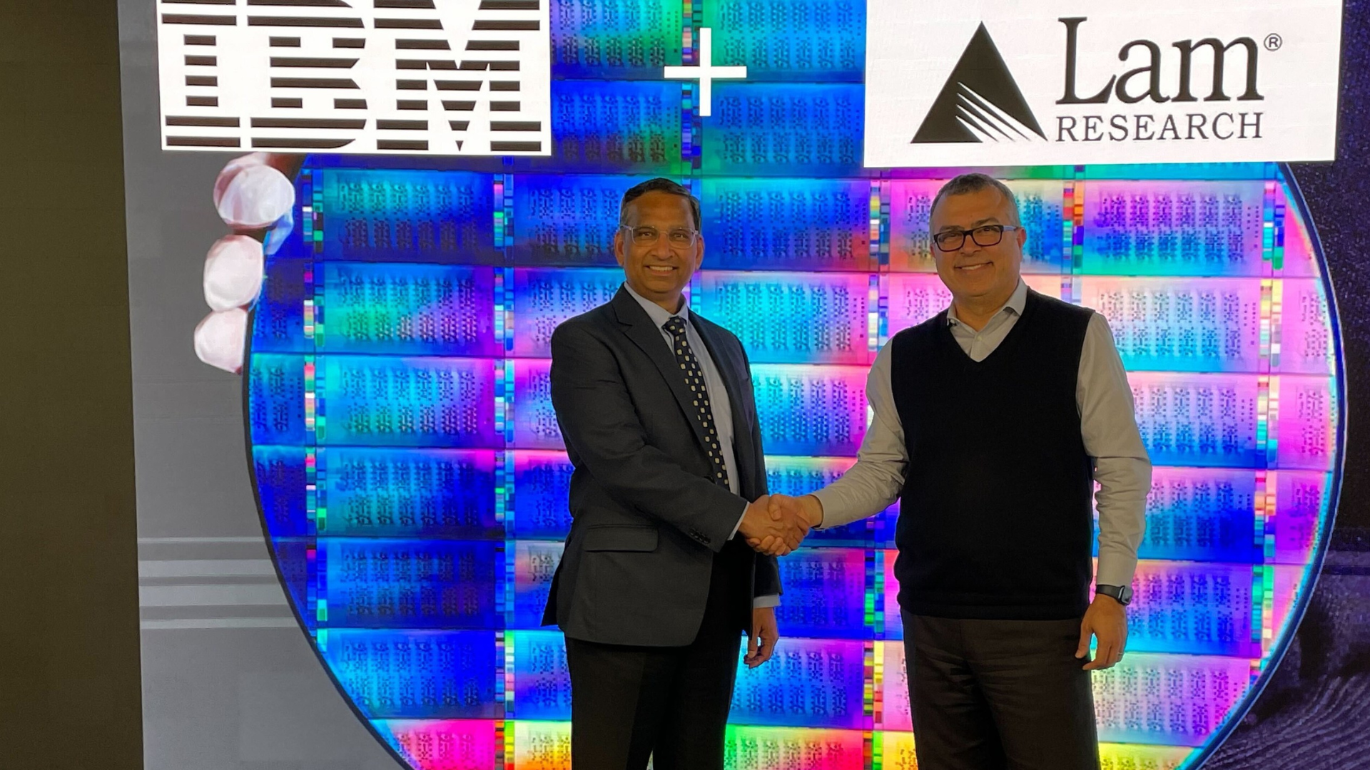
IBM and Lam Research Team Up on High NA EUV Dry Resist to Push Chip Scaling Past 1nm
Key Facts
- What: IBM and Lam Research announced a five-year collaboration to develop materials and processes for scaling logic chips beyond 1nm using High NA EUV lithography and Lam's Aether dry resist technology.
- Where: Research will take place at IBM Research's facilities at the NY CREATES Albany NanoTech Complex in Albany, New York.
- Focus Areas: Validation of full process flows for nanosheet and nanostack device architectures, backside power delivery, and reliable pattern transfer with high yield.
- Technology Edge: Lam's Aether dry resist absorbs 3-5 times more EUV light than traditional carbon-based resists, enabling lower exposure doses and single-print patterning at advanced nodes.
- History: The companies have collaborated for over a decade on 7nm processes, nanosheet transistors, and early EUV integration, including IBM's 2nm node chip unveiled in 2021.
IBM and Lam Research have launched a five-year partnership to overcome the technical barriers to scaling logic devices below 1nm, focusing on High Numerical Aperture Extreme Ultraviolet (High NA EUV) lithography and next-generation dry resist materials. The work, centered at IBM's Albany NanoTech Complex in New York, aims to validate complete process flows for advanced 3D transistor architectures and backside power delivery while addressing the yield challenges that have slowed adoption of High NA EUV tools.
The collaboration builds on more than ten years of joint development between the two companies. Their previous efforts contributed to 7nm process technology, the introduction of nanosheet transistor architectures, and early integration of EUV lithography. In 2021, IBM unveiled what it called the world's first 2nm node chip as part of that ongoing partnership.
High NA EUV lithography represents the next major leap in chip patterning, promising finer resolution than current EUV systems. However, conventional chemically amplified resists — wet-process materials applied via spin-coating — struggle with the tighter tolerances and stochastic effects at these dimensions. Lam Research's Aether dry resist technology offers a promising alternative by using vapor-phase precursors deposited in a dry process and developed with plasma-based dry techniques.
According to the joint announcement, Aether's metal-organic compounds absorb three to five times more EUV light than traditional carbon-based resists. This higher absorption reduces the exposure dose required per wafer, helping maintain single-exposure patterning instead of costly multi-patterning steps at sub-1nm nodes. The dry nature of the process also reduces the number of steps between exposure and etch, minimizing opportunities for pattern degradation at the extremely fine geometries required for future logic devices.
The partnership will leverage several of Lam's advanced platforms, including the Kiyo and Akara etch systems, Striker and ALTUS Halo deposition tools, and the Aether dry resist process. Teams will work to build and validate full process flows for both nanosheet and emerging nanostack device architectures alongside backside power delivery technology. Backside power delivery routes electrical power through the rear of the wafer, freeing up valuable front-side interconnect layers for signal routing and improving overall performance and density.
"Together, these capabilities are aimed at allowing High-NA EUV patterns to be reliably transferred into real device layers with high yield and enabling continued scaling, improved performance, and viable paths to production for future logic devices," the companies stated in their press release.
The yield-at-transfer challenge is particularly critical. As features shrink below 1nm, even minor variations in pattern fidelity can lead to significant yield loss. Lam's dry resist approach is designed to provide better process control and stability compared to traditional wet resists, which can suffer from line edge roughness and other stochastic issues amplified by High NA EUV's higher resolution.
In January, Lam announced that Aether had been selected by a leading memory manufacturer as the production tool of record for its most advanced DRAM processes, though the manufacturer was not named. The new collaboration with IBM extends the technology's application into leading-edge logic devices, an area historically dominated by foundries such as TSMC, Samsung, and Intel.
Competitive Landscape and Industry Context
The announcement arrives as the semiconductor industry faces mounting pressure to continue scaling despite the growing physical and economic challenges of Moore's Law. High NA EUV tools from ASML, which feature a 0.55 numerical aperture compared to 0.33 in current EUV systems, are expected to be essential for nodes at 2nm and below. However, the full ecosystem — including resists, deposition, etch, and metrology — must evolve in parallel.
IBM has positioned itself as a research leader in advanced semiconductor technologies, even as it exited volume manufacturing years ago. Its Albany NanoTech Complex serves as a key hub for pre-competitive research, often partnering with equipment suppliers and other chipmakers to develop technologies that eventually flow into commercial production.
For Lam Research, the partnership represents an important validation of its Aether dry resist platform in the logic space. As AI workloads drive explosive demand for more powerful and efficient processors, the ability to produce smaller, faster, and more power-efficient chips becomes increasingly critical. Sub-1nm logic devices could enable significant gains in performance per watt, crucial for both data center AI accelerators and mobile/edge applications.
Impact on Developers, Users, and the Industry
The collaboration could accelerate the timeline for commercial High NA EUV adoption in logic manufacturing. By focusing on full process integration rather than isolated tooling, IBM and Lam aim to deliver proven flows that foundries can more readily implement in production environments.
For chip designers and system architects, successful scaling below 1nm would unlock new levels of transistor density, potentially enabling larger AI models to run more efficiently or allowing entirely new architectural approaches. Improved backside power delivery, combined with nanosheet and nanostack transistors, could deliver meaningful gains in both performance and power efficiency.
The industry as a whole stands to benefit from diversified innovation in the EUV ecosystem. While ASML holds a monopoly on High NA EUV scanners, the materials and process technology developed through this partnership could help reduce dependency on any single supplier and improve overall manufacturing yields.
What's Next
The five-year timeline suggests initial research results may emerge within the next 12-24 months, with more substantial process validation likely in years three through five. The companies have not disclosed specific node targets or commercialization timelines, but the stated goal is to enable viable production paths for sub-1nm logic devices.
Success in this collaboration could influence the broader roadmap for 1nm-class and Angstrom-era process technologies. Foundries are already planning their High NA EUV insertion points, and proven dry resist solutions could accelerate those plans while reducing the technical risk.
As the industry enters what the partners describe as "a new era of 3D scaling," rethinking materials and processes has become essential. Progress at these dimensions increasingly depends on close collaboration between research organizations, equipment suppliers, and eventual manufacturing partners.
Sources
- Tom's Hardware - IBM and Lam Research team up on High NA EUV dry resist to push chip scaling past 1nm
- IBM Newsroom - IBM and Lam Research Announce Collaboration to Advance Sub-1nm Logic Scaling
- PR Newswire - IBM and Lam Research Announce Collaboration to Advance Sub-1nm Logic Scaling
- StockTitan - IBM and Lam team up to shrink chips below 1nm for AI-era power